- Joined
- Jan 14, 2011
- Messages
- 75,850
- Location
- Gillette, Wyo.
- Tagline
- Halfbiass...Electron Herder and Backass Woof
Nice work Glen!!

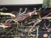
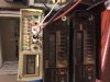
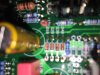
Gee Ron I thought was pretty cleanMan, that looks like a bitch to work on. Looks like a pile of wire piled on a pile of wires
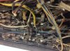
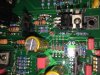
More photos
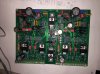
Thank you Dennis. I guess I have looked at it long enough that I can get to any thing easily. I can fold the back plane away from the chassis to get at everything.Fantastic job Glen. You have a one of a kind amp - or is that a pair of a one of a kind. The backplane is quite busy but you did a very nice job in getting everything routed well. You'll need to let us know how they sound compared to the upgraded 700s - cool stuff.
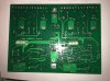
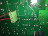
I have checked it over. Looks good to me. Please look and see if anything is different between channels
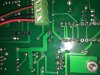
Thank you JoeDo you have a solder splash between anode of D3R and D2R?? Topside of board.
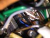
I have removed wire 6 and 7 to Q6 and bias transistor
checked R21 and R20 R9 and R31 all good
Checked D1-D4 all good
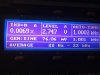
voltage is
6.7 at collector
2.5v olts at base
1.4 volts at emitter
somewhere voltage is leaking in close to the collector
more to come
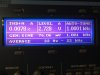
Ok I will check out the other half. That does seem like a good possibility.Hi Glen
The emitter voltage should be negative if you have 0.000 at the output. Something to check.
Seems like the bottom half is possibly not pulling at all Glen.
Ok I will check out the other half. That does seem like a good possibility.
Will report back with better data
Gee Ron I thought was pretty clean
Here is what looked like at the start
Ron your assessment was correct the first time. It is Busy and caused my latest miss adventure.I meant that that is a lot of stuff packed in. I admire you being able to take this monster and bring it back to life. Maybe someday I will come across one!