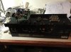
I am working out the last items on my list
One of the things is the protection circuit.. In the following description of Bob's patent for this circuit as used in the series one amp, and it appears to run throughout all the series, the system is described in great detail. The missing factor is what the settings for the protection circuit are set to. Can anyone address this as to fine tuning these amps for different rail voltages, etc. In this 500 i though of adding a variable resistor in place of the 180 ohm base resistors R114 and R126. I believe this was done back in the day for the Kelly Deyong Amps but cannot remember if was for more protection or to milk a little more juice out of them.. I have often wondered if the protection circuit kicking in effects the clipping ..
If anyone has a clear explanation for how this circuit work other than what follows please post it
Glen
From the patent
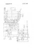
FIG. 1, is an overall electrical circuit diagram of a direct coupled, dual channel, solid state amplifier, incorporating energy limiting safety circuit portions; and
FIG. 2 is the enlargement of circuit portions serving as energy limiting safety or protection circuit components for one channel, which is part of the overall electrical circuit of the dual channel high fidelity amplifier illustrated in FIG. 1, where two such groups of energy limiting circuit components are illustrated.
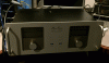
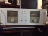
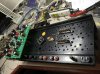
DESCRIPTION OF PREFERRED EMBODIMENT Amplifier Circuit Components The high fidelity amplifier 10, illustrated in FIG. 1, with some of its energy limiting protection circuit components illustrated again in FIG. 2, is a direct coupled, solid state, dual channel, class B, linear amplifier capable of producing 700 watts of power, root mean square, when each channel is terminated in}! ohms, complex or resistive. It is capable of producing 350 watts per channel from 0 Hz to 20kI-lz. It may safely operate into any passive load whose complex impedance may range from zero to infinity. The input signal to be amplified is received by the normal, or by the direct coupled input. The signal is transmitted by transistor Q1 to the top of potentiometer R1. The wiper arm of R1 adjusts the amplitude of the signal to be applied to the base of transistor Q2. Transistors Q2 and Q3 form a voltage differential amplifier also consisting of transistors Q4 and Q5. Transistor Q7 is driven by transistor Q4. The collector of transistor 07 may swing the full supply voltage. The output of transistor O7 is applied to the bases of transistor Q8 and Q11 so a complimentary emitter follower action takes place and the output at the emitters of transistors Q8 and Q11 may swing the full voltage supply. Transistor Q6 provides a means of maintaining a stable bias voltage for the output transistors. Diodes D3, D4, and D provide a small for ward voltage at the base of transistor Q6, which causes 'it to turn on and maintain a constant voltage between its emitter and collector terminals regardless of the amount of the collector current. Potentiometer R2 permits a small adjustment of this otherwise constant voltage to be made in order that the output transistors may be rendered conducting on receipt of a signal as small as one pleases.
Feedback voltage taken from the output C of the amplifier is applied to the input differential amplifier having transistors Q2 and Q3. This feedback voltage reduces the overall distortion as measured at the output terminal of the amplifier 10.
The output stage of the amplifier 10 consists of six output transistors, Q14 Q19, two driver transistors, Q12 and Q13, and the two complementary emitter followers transistors Q9 and Q10. As viewed in FIG. 1, the upper output transistors are operated as emitter follower transistors; the lower output transistors are operated as common emitter amplifier transistors. Unity voltage feedback is applied through resistor R3 to the emitter of transistor Q11 so the forward voltage gain assumes a value of one for the combination of transistors O11, O13, Q15, Q17 and Q 19.
Energy Limiting Protection Circuit Components These groups of output transistors in each of the dual channels must be protected and the components of the overall circuit added to provide this protection as shown in FIG. 1 and some as shown in FIG. 2 are the transistors Q9 and Q10, and diodes D6, D7, D8, and D9. They form the active circuit components of the energy limiting protection circuits 12, one for each channel which limit the total energy retained by the output transistors to a safe and pre-determined maximum. These protection circuits 12 are necessary to insure that output transistors will not fail in the event the amplifier overall circuit 10 is accidentally overloaded. The operation of each protection circuit 12, in reference to FIG. 2, where one protection circuit for one channel is illustrated, is as follows. The energy limiter protection circuit 12 develops an output voltage which is an analog representation of the instantaneous silicon chip temperature of the output transistors. When this analog voltage reaches a predetermined threshold, which represents the output device silicon chip temperature and tracks with the energy absorbed, the limiter circuit 12 shunts the drive current around the first driver transistors, thereby preventing the output transistors from experiencing excursions into their unsafe operating region. Current I, which is flowing through resistor R9, develops a voltage across it which is applied to the wiring summing junction A through resistor R8. The time derivative of current I, dI/dt, is generated by utilizing the capacitor C3 and it is made effective also at the wiring summing junction A.
The time integral of I, Idt, is functionally generated by the combination resistor R7 and capacitor C1 and it is made effective also at the summing junction A by resistor R6. Resistor R10 and switching diode D8 form an integrator reset function by discharging capacitor C1 during negative half-cycles of the waveform of the output circuit portions. Resistor R5 provides a voltage, V, at the wiring summing junction A, which is directly proportional to the voltage across the output transistors or the amplifier output. Since the wiring summing junction A is isolated from the integrating capacitor C1 by resistor R6, a portion of this voltage appears at the I junction of resistor R6 and resistor R7 and is integrated by capacitor C1. The value of the total integral is, to a first approximation, the value of Vldt, where the limits of integration are chosen to be over one half cycle of the waveform, or by R7Cl seconds, whichever occurs first. If the half period of the waveform is less than R7Cl seconds, the ongoing integration will be stopped by the reset function. If the half period is longer than R7C1 seconds, the integration is stopped when capacitor Cl becomes fully charged at approximately, R7Cl seconds. The electrical time constant, R7Cl seconds, is chosen to be approximately the same as the thermal time constant of the silicon. chip in each output transistor.
Resistor R4 and capacitor C5 develop a voltage which appears at the wiring summing junction A and is the time derivative, dv/dt, of the output voltage. This causes limiting of the output at extreme dv/dt rates, such as occurs during high frequency clipping. If the value of any of these voltage quantities, or their sum, exceeds the threshold VBE of transistor, Q9, it turns on, and thereby activates diode D6, whose anode is connected to the base of transistor Q8. This overload? ing sensing action shunts the drive current away from transistor Q8, preventing any further increase in energy absorption by the output transistors. Consequently, amplifier 10 having energy limiting circuit components provides as much power as other amplifiers having or requiring three times as many output transistors, when protection is obtained either through use of current limiting or power limiting circuit components.