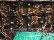
PL400 II Resurrection

Joined
Jul 30, 2019
Messages
97
Location
Belgium
#81
Gepetto, why did you use different identifiers for the drivers on the connection diagrams vs. the PL schematics ?
And is there a way to test the board without the power to the drivers connected ?

Thanks, Peter
 

Gepetto

Administrator
Staff member
Joined
May 15, 2011
Messages
13,553
Location
Sterling, MA
Tagline
Old 'Arn Enthusiast
#82
PL has many schematics Peter with different nomenclature on each. It drives you nuts trying to keep up with all the versions that they had.

Yes there is a thread recently posted by Mark Lucitt where I explain how to test for functional control board (safe launch) without connecting the output drivers.
 
Joined
Jul 30, 2019
Messages
97
Location
Belgium
#84
Good news and bad news.
Powered up without fuses, no smoke. Powered up with fuses, no kaputt fuses or smoke. No DC on outputs.. No sparking drivers. Channel L biased perfectly and rock solid as 375mV, right however was down at somewhere around 30 mV. Turning the bias trimmer showed the circuit worked as I could get it up to 60mV. So I suspected a transistor. I got back to measuring around the fire source (the repair I made around the diode worked) and measured Q7 (OK) and Q8 (not so OK) I decided to take it out and measuring again to be sure, but unfortunately one of it's legs broke when removing it. That together with the fact that diode and resistor behind it took the brunt of the initial short I'm pretty sure I've got the right part. Unfortunately I don't have one.

But I'm getting there.
 
Joined
Jul 30, 2019
Messages
97
Location
Belgium
#86
I've swapped Q8L to right, no change. I'm now fresh out of ideas. The only thing I haven't been over is that opamp. I think I've don all transistors, diodes and some of the passive components as well as the pathways. I'm going to sit tight until Gepetto comes along.

Peter
 

Gepetto

Administrator
Staff member
Joined
May 15, 2011
Messages
13,553
Location
Sterling, MA
Tagline
Old 'Arn Enthusiast
#87
What voltage are you measuring from C-E on Q6 the bias transistor? Compare to your good channel. Since you have a perfectly good channel, use that to find areas where you have anomalous voltages. Doubtful on op amp if the output is zero. Op amp has zero to do with bias.
 
Joined
Jul 30, 2019
Messages
97
Location
Belgium
#88
Oh sorry, forgot to mention that, IIRC it’s 2.03V on the left bias adjusted to 375 mV) and 1.99V on the right, unadjusted. I have transplanted the good q8 to the right. So no complete left. peter
 

Gepetto

Administrator
Staff member
Joined
May 15, 2011
Messages
13,553
Location
Sterling, MA
Tagline
Old 'Arn Enthusiast
#89
So if you have C-E or 2.03V on the left when adjusted to 375mV and 1.99 on the right, your bias is working fine.

Check the base of Q6R and Q9R and compare to the working left channel voltages. Check the collector of Q6R and Q9R and compare to your working left channel.
 
Joined
Jul 30, 2019
Messages
97
Location
Belgium
#90
Something is funny. I replaced D13R. In front of D13 there’s a resistor. If I measure the left channel that resistance in series with D13 it starts at a few kOhm and stabilises around 12 kOhm. On the right it shoots up and stabilises around 258 kOhm. I’m sure that’s telling me something...
 

Gepetto

Administrator
Staff member
Joined
May 15, 2011
Messages
13,553
Location
Sterling, MA
Tagline
Old 'Arn Enthusiast
#92
Left : q6 1.11, q9 -0.7, right q6 0.6, q9 - 1.22 Cheers, Peter
How about the corresponding collector readings for same 2 devices Q6 and Q9 both channels?

You are getting close. Something is not right with Q6R OR its downstream driver device.
 

Gepetto

Administrator
Staff member
Joined
May 15, 2011
Messages
13,553
Location
Sterling, MA
Tagline
Old 'Arn Enthusiast
#94
Don't replace it before you check the collector readings. My suspicion has not centered around Q6R being bad.
 
Joined
Jul 30, 2019
Messages
97
Location
Belgium
#98
It turns out that when I received the info package from Joe there was a schematic in it ! Had to replace D13L, and the 30 mV I measured before has now dropped to near as makes no difference 0 when measuring on the bias check point. Now I got the schematic I can do some more investigating but need to figure out how the circuit works.
I think I’m looking at this ass backwards...
 
Last edited:
Joined
Jul 30, 2019
Messages
97
Location
Belgium
#99
I've replaced the transplanted MPS751, so both channels are now once more complete. Help on how to proceed is very much appreciated.

The last measurements taken were

Collectors Q6l 78, q9l - 0,86, q6r 78, q9r -0,66.

Pete
 

Gepetto

Administrator
Staff member
Joined
May 15, 2011
Messages
13,553
Location
Sterling, MA
Tagline
Old 'Arn Enthusiast
I put all the questions and answers into one post rather than spread over multiple responses.

You answered: Oh sorry, forgot to mention that, IIRC it’s 2.03V on the left bias adjusted to 375 mV) and 1.99V on the right, unadjusted.

I commented: So if you have C-E or 2.03V on the left when adjusted to 375mV and 1.99 on the right, your bias is working fine.


Question asked: Check the base of Q6R and Q9R and compare to the working left channel voltages. Check the collector of Q6R and Q9R and compare to your working left channel.

You answered: Left : q6 1.11, q9 -0.7, right q6 0.6, q9 - 1.22 Cheers, Peter


Question asked: Don't replace it before you check the collector readings. My suspicion has not centered around Q6R being bad.

You answered: Q6l 78, q9l - 0,86, q6r 78, q9r -0,66. I’m really curious now


Next questions: What is the reading of the emitter on Q6L/R and Q9L/R? The pinout on these devices is B-C-E looking at the face of each device when leads are pointed down. Please confirm this was the convention used for reporting the above results.
 
Top