Barn Find PL400

Are you sure that when you found this barn find that the board had not been worked on prior to you finding it? The reason I ask is that the photos of the same board you have installed is also shown in a photo by poster GMEAD today and it shows the orientation of Q1-Q4 differently than your situation. Have you traced the etch to the schematic to ensure proper placement of devices? I would do that except that I gave away all my original PL wind chime mobiles quite some time ago. Good to check and confirm.
 
Last edited:
I know exactly what you are talking about. It’s a real head scratcher. The board is printed with the devices pictured opposite their placement. Also the hole pitch is triangular as are the device leads. As I have them installed I had to bend the center lead forward to correct for the mistake in the board design. As I know you are aware the 97 is a C-B-E pin out. As installed the emitters have continuity and are 220k from the negative bus.

Also, I’m listening to Dire Straights now (how’s that for irony) and the amp performs as expected (Once started without load). I think we can say with certainty that it would not pass a signal with Q1 and Q2 image.jpgimage.jpginstalled backwards.
 
If those are the original TIS97 back in place, that looks correct, it is more the difference in Q3-Q4 that should be confirmed.

Transistors with E-B-C and C-B-E pinouts can be installed reversed and appear to work.
 
You can see the trace that encircles Q1 and Q2. In the photo it’s Q2 on top and Q2 on bottom.image.jpg
 
Oh, I see. I missed your point at first. I’ll look into Q3 and Q4 placement and get back to you.
 
The photo here is upside down from the drawing with Q4 over Q3. On Q4 we see the left pin trace to to Q5 in the center of the board, so that pin is the collector, right. Collectors on the bottom of a PNP. Q4 is an A93 and EBC. That divide is installed with pin 3 on the left and pin 1 on the right.

Q3 has a collector to ground. Follow the right pin to the diodes on the ground trace. Q3 is a TIS-93, CBE. Pin 1 is on the right.

with both pin 1 on the right, they shouldn’t be face to face or back to back, they should be aligned the same.

the board designer didn’t think so, judging from the pin hole locations. Where is my mistake?
IMG_1834.jpeg
 
Your soldering skill on this ancient printed circuit board is nothing short of amazing.
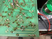
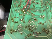
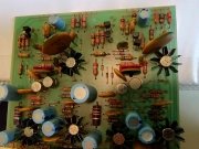
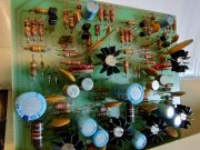
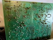
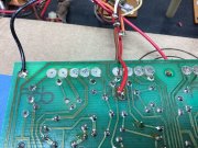
I have an original unmolested Phase Linear 14B Board. Comparing them with the above pictures shows no irregularities. This one has pairs of GES 97, and GES 93/MPS 93. You can have this P14B Board if you want it.PL14B 1.jpg

PL14B 2.jpg

PL14B 3.jpg

PL14B 4.jpg

I hope these pictures can help.
 
Last edited:
You may want to try lifting one end of both D9 and D10 to disable the protection circuit to see if it is complicit with the bring up problems with a load attached.

If it comes up properly with a load attached and with these diodes lifted, you will have a good indication that the protection circuit is part of your issue.
 
Your soldering skill on this ancient printed circuit board is nothing short of amazing.
I have an original unmolested Phase Linear 14B Board. Comparing them with the above pictures shows no irregularities. This one has pairs of GES 97, and GES 93/MPS 93. You can have this P14B Board if you want it. I hope these pictures can help.

Thanks for the compliment. I just bought a hakko 472D rework station and I could not do this kind of work without it. I see your Q3 and Q4 are installed as mine. Phase Linear must have had board revisions for which we do not have documentation. I’ll send you a PM about the board. I’m likely to by a White Oak board but I’d like to swap out another board to see if my problem is off board. Truthfully, it‘s more about the journey than the destination for me. I like the puzzle.
 
You may want to try lifting one end of both D9 and D10 to disable the protection circuit to see if it is complicit with the bring up problems with a load attached.

If it comes up properly with a load attached and with these diodes lifted, you will have a good indication that the protection circuit is part of your issue.

That sound like a good plan. Thanks.
 
You may want to try lifting one end of both D9 and D10 to disable the protection circuit to see if it is complicit with the bring up problems with a load attached.

If it comes up properly with a load attached and with these diodes lifted, you will have a good indication that the protection circuit is part of your issue.

Okay, I lifted both sets and the problem persists. If I understand correctly, this suggest the problem is not with the Gremanium transistors or the network to the right of them on the drawing. The bias circuit works as expected and Q6 tested well a week ago. I’m thinking I should focus on Q7 and Q10, but I wonder if that is realistic since the amp plays once started.

Is it a bad idea to run the amp with those diodes lifted?
 
Good that you ruled that out as a culprit. For safety's sake, I would recommend reattaching the lifted leg on each diode.
 
Gepetto

In the latched condition they are slightly negative.

Left
Q1 is -.501 and
Q2 is -.571

Right

Q1 -.496 and
Q2 -.560

Operating unlatched the collectors are both at about 20v. I don’t see Q1 much lower than Q2. About 50mv difference.
Edit: I’d expect the parallel reversed diodes on the collectors to keep the collector voltages very close.

What transistor has been used successfully as a TIS97 substitute? I don’t have an TIS97 but I do have some matched 2sk470s.
These voltages make little sense given that R4 || R7 is 165K and R6 is 220K. Average Q1-Q2 collector voltage should be in the vicinity of 11.5V unless the B+ rail is severely sagging when in this latch up condition.
 
These voltages make little sense given that R4 || R7 is 165K and R6 is 220K. Average Q1-Q2 collector voltage should be in the vicinity of 11.5V unless the B+ rail is severely sagging when in this latch up condition.

It is sagging under the DBT. And B+ sags more than B-. About 10+ and 24- IIRC.
 
Today I’m listening to Dickie Betts on the Barn Find PL400 off the DBT. I’m doing a short victory lap.

Mark, I got the PL14B and it is indeed sweet. It does indeed look to be a virgin. I went through it part by part checking all the resistors, caps, diodes and transistors and found not a single problem. Next I set it side by side with my snake bit board and checked everything on that board again against the virgin board. I couldn’t find a single discrepancy which surprised me greatly. I really wanted to find a smoking gun but did not. Instead I installed the virgin board and lit it up on the DBT with a load. No problems; it passes a nice waveform, both channels equal, DC offset a bit high but tolerable (Under 50mv). Most importantly it does not blow fuses when started with a load. I’m still waiting for the protection relay to arrive before I move it to the main rig but it sounds about right on the baby advents; the only speakers I trust it with at this point.

I took the amp all the way back to stock for the new board tryout. The next steps after the protection relay board are to methodically replace the filter caps, recap the virgin board and find some matched TIS-97 for the DC offset. Unfortunately it will need to wait as I’m off on a big road trip tomorrow. A big thank you to everyone who offered their time, advice and good wishes. Be well.IMG_1840.jpeg
The virgin board inspected, cleaned and ready for installation.
 
sounds a lot like christine....tried and tried...tested and tested....could prove nothing...
put in pl20...been playing ever since!!!!
sometimes you gotta do what you gotta do!!!
congratulations!!!!
they do sound nice, dont they!!!
 
Back
Top