
400 S2 - Wopl In Progress
- Thread starter 74sdta
- Start date
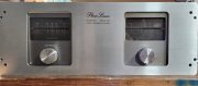
Looking at the photos, it appears the amp was mounted in a rack, and the matching rack handles were removed. Hopefully you still have them. The good thing is whoever installed the amp in the rack didn’t butcher the front panel.
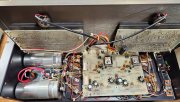
The driver board is in pretty good shape, given its age there’s no scorching on the left side of the board where the power supply is located. The 7.5 K 2 watt resistors on the driver board are failure prone. When they open up, the amp goes DC on the output, If you intend to keep this driver board at a minimum replace those two resistors
There are a couple capacitors on the display boards that tend to open up. The lowest cost solution is to replace all the electrolytic capacitors on the boards. The alternative is upgrade to the white oak display boards.
Yes, this unit did not have that nasty crap.
As of now, the unit has been blown apart and the xfmr, p-straps are set aside. The heatsinks have been prepped and sit on the bench with the WO chassis.
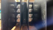
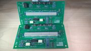
I have not melted any solder in a looooog time, so I thought I would start with the WO LED boards as a warm-up. Completed boards;
Now off to see if my station is up to the backplane PEM nut work.
As of now, the unit has been blown apart and the xfmr, p-straps are set aside. The heatsinks have been prepped and sit on the bench with the WO chassis.
I have not melted any solder in a looooog time, so I thought I would start with the WO LED boards as a warm-up. Completed boards;
Now off to see if my station is up to the backplane PEM nut work.
- Joined
- Nov 1, 2014
- Messages
- 3,250
- Location
- Gaston, SC
- Tagline
- Victim of the record bug since age five
Update - not much progress since dogs were occupying garage due to weather. Ordered misc. parts and cleaned up both ends of transformer.
View attachment 79643
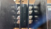
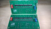
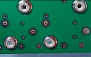
Started backplane work today. Review from the pros - does this look good?
View attachment 79644
View attachment 79643
Started backplane work today. Review from the pros - does this look good?
View attachment 79644
Update - not much progress since dogs were occupying garage due to weather. Ordered misc. parts and cleaned up both ends of transformer.
View attachment 79643
Started backplane work today. Review from the pros - does this look good?
View attachment 79644
View attachment 79643
Started backplane work today. Review from the pros - does this look good?
View attachment 79644

- Joined
- Nov 1, 2014
- Messages
- 3,250
- Location
- Gaston, SC
- Tagline
- Victim of the record bug since age five
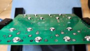
I agree with the guys, a little blurry but those two that are in focus look like they are not soldered on the back side, is this right? LOTS of heat and solder as this is a HIGH POWER connection.
It’s also a high stress area- they hold both the transistors and the heatsinks in place, the heatsinks often become a “grab point” when you go to lift it. That being said, be careful with transistor installation, overtightening can pierce the silpads giving rise to a short circuit. A delicate balance…
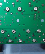
Thanks for the better view but again, maybe it is a shadow or some flux but these areas look a little suspect
View attachment 79653
But let's see what the real experts have to say...
View attachment 79653
But let's see what the real experts have to say...