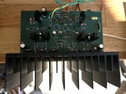
I purchased a PL300 in need of repair. I thought the build quality was pretty marginal so I decided to redesign the board rather than repair what I had. I modified the driver and bias circuitry and then after doing some testing I changed the output devices to lateral MOSFETs.
The stock heat sink looks large but based on the temperature rise it's actually undersized for the 125 watt output rating. I can bias the lateral FETs at a lower quiescent current (70 mA/device) and the heat sinks don't get nearly so hot.
My breadboard testing worked out very well so I decided to make a circuit board. I laid the board out with KiCAD. It's a 4 layer board with 1 ounce copper power power and return planes.
I've used it at least 4 days a week for the last couple months and I'm very happy with how it turned out.
The stock transformer voltage drops off quite a bit under load but I was able to get 132 watts out with a THD of 0.005% at 20 KHz and 0.0015% at 2 KHz. That meets or exceeds the original ratings.
The stock heat sink looks large but based on the temperature rise it's actually undersized for the 125 watt output rating. I can bias the lateral FETs at a lower quiescent current (70 mA/device) and the heat sinks don't get nearly so hot.
My breadboard testing worked out very well so I decided to make a circuit board. I laid the board out with KiCAD. It's
 a 4 layer board with 1 ounce copper power power and return planes.
I've used it at least 4 days a week for the last couple months and I'm very happy with how it turned out.
The stock transformer voltage drops off quite a bit under load but I was able to get 132 watts out with a THD of 0.005% at 20 KHz and 0.0015% at 2 KHz. That meets or exceeds the original ratings.
