Published this document earlier in one of the long threads and it is now buried somewhere in those archives. Bringing it to its own thread to make it easier to find.
Description of the latch up possibility.
When power is applied to the PL amp, the +/- bulk caps charge rapidly to provide the main power for the amp. During this start up phase, the critical ‘front end’ long-tailed pair formed by the differential amp (Q1 and Q2) is not in control yet because it is not provided sufficient voltage to properly bias itself and operate as an op amp. In addition, the positive and negative main rails do not rise at exactly the same rate leading to bias imbalance in this front end during this critical start up period.
Before the front end can control the amp output using global negative feedback provided from the output through R15, R13 and C6, the tendency is for the amp to come up with a positive bias on the output. This is because the positive rail feeds directly through R17 then through R18 then through the base emitter junction of Q10, turning it on quite hard on power up which in turn drives Q11, Q13, Q15, Q17 to turn on quite hard. This DC voltage is fed back through R15, R13 to begin charging C6 in the positive direction. During this startup phase, Q5 is not active yet (off) because the front end is not biased properly and cannot control the second stage current amplifier formed by Q3 and Q4 to provide base current to control Q5.
If the amp starts properly and the front end comes into regulation fast enough, the global negative feedback compensates for this and through the action of the differential front end turns on Q4 and in turn Q5 to bring the positive turn on bump back to ground again and all is well.
In the latch up condition, this start up process begins but then runs away as follows. Q10, Q11, Q13, Q15, Q17 all turn on hard due to the bias from R17 and R18. This positive bump produces a current in R15 and R13 starting to slowly charge C6. The rapid voltage rise at the nodal junction of R15 and R13 starts a current flowing through R10 and C4 into the base of Q2. This base current due to both +/- rails starting up at similar rates will flow through both the base-emitter junction (into R6) as well as the base-collector junction (into R7). The split of current flow is somewhat indeterminant but the base-collector junction is typically a few millivolts lower than the base-emitter junction in a TIS97 transistor. As a result, the tendency will be for this feedback current to flow through the path of least resistance, the base-collector junction and into R7. This is not the intent by design. This action produces a cut off of Q4, the MPSA93 transistor which continues to hold off Q5 which reinforces the continued rise of the output voltage in the positive direction. Essentially negative feedback turns into positive feedback by accident, the amp latches up and the output rail goes to the positive rail. In the case of the PL20 board with the +/-20V regulators for the front end, once the amp is latched up, the collector of Q2 rises to approximately 29V turning off Q4 very hard, giving the amp no chance of coming back into regulation. This collector node of Q2 is nominally supposed to operate at 10V. If the amp is latched up and then power cycled rapidly again, C6 will have retained much of this ~29V charge causing the amp to almost guarantee to latch up again.
How do the back to back diodes around C6 fix this?
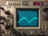
It is mainly the diode with its anode connected to the positive side of C6 and its cathode connected to the negative side of C6 that does the trick. The other diode is added for symmetry even though the amp has no propensity to latch up in the negative direction. This first diode clamps the node at the junction of R15 and R13 to a maximum of +/- 2.36V for the PL400 or +/- 2.85V for the PL700B. This allows the front end to become properly powered and stabilized and keep the negative feedback signal within the allowable common mode voltage range of this front end stage. Any tendency to latch up will be quickly remedied once the +/- 20V supplies come into regulation. These diodes do not come into play when the amp is amplifying audible frequencies as the impedance of C6 is so low (for example, at 20Hz its impedance is only 79 ohms and will only experience 0.49V peak when the amp is producing a 80V peak signal output which is less than the Vf of the diodes involved, at 40Hz there is only 0.25V peak across C6 and so on). This is an elegant and effective fix and allows the amp to be power cycled rapidly with no concern of latch up.
What about turn on and turn off thump? These are actually artifacts of the front end not being in control during turn on and turn off. If these thumps exist, it is evidence that the amp is starting to latch up and then recover. This fix allows the negative feedback signal to more rapidly work with the front end to stabilize and regulate the output by staying well within the common mode range of the front end.
Description of the latch up possibility.
When power is applied to the PL amp, the +/- bulk caps charge rapidly to provide the main power for the amp. During this start up phase, the critical ‘front end’ long-tailed pair formed by the differential amp (Q1 and Q2) is not in control yet because it is not provided sufficient voltage to properly bias itself and operate as an op amp. In addition, the positive and negative main rails do not rise at exactly the same rate leading to bias imbalance in this front end during this critical start up period.
Before the front end can control the amp output using global negative feedback provided from the output through R15, R13 and C6, the tendency is for the amp to come up with a positive bias on the output. This is because the positive rail feeds directly through R17 then through R18 then through the base emitter junction of Q10, turning it on quite hard on power up which in turn drives Q11, Q13, Q15, Q17 to turn on quite hard. This DC voltage is fed back through R15, R13 to begin charging C6 in the positive direction. During this startup phase, Q5 is not active yet (off) because the front end is not biased properly and cannot control the second stage current amplifier formed by Q3 and Q4 to provide base current to control Q5.
If the amp starts properly and the front end comes into regulation fast enough, the global negative feedback compensates for this and through the action of the differential front end turns on Q4 and in turn Q5 to bring the positive turn on bump back to ground again and all is well.
In the latch up condition, this start up process begins but then runs away as follows. Q10, Q11, Q13, Q15, Q17 all turn on hard due to the bias from R17 and R18. This positive bump produces a current in R15 and R13 starting to slowly charge C6. The rapid voltage rise at the nodal junction of R15 and R13 starts a current flowing through R10 and C4 into the base of Q2. This base current due to both +/- rails starting up at similar rates will flow through both the base-emitter junction (into R6) as well as the base-collector junction (into R7). The split of current flow is somewhat indeterminant but the base-collector junction is typically a few millivolts lower than the base-emitter junction in a TIS97 transistor. As a result, the tendency will be for this feedback current to flow through the path of least resistance, the base-collector junction and into R7. This is not the intent by design. This action produces a cut off of Q4, the MPSA93 transistor which continues to hold off Q5 which reinforces the continued rise of the output voltage in the positive direction. Essentially negative feedback turns into positive feedback by accident, the amp latches up and the output rail goes to the positive rail. In the case of the PL20 board with the +/-20V regulators for the front end, once the amp is latched up, the collector of Q2 rises to approximately 29V turning off Q4 very hard, giving the amp no chance of coming back into regulation. This collector node of Q2 is nominally supposed to operate at 10V. If the amp is latched up and then power cycled rapidly again, C6 will have retained much of this ~29V charge causing the amp to almost guarantee to latch up again.
How do the back to back diodes around C6 fix this?
It is mainly the diode with its anode connected to the positive side of C6 and its cathode connected to the negative side of C6 that does the trick. The other diode is added for symmetry even though the amp has no propensity to latch up in the negative direction. This first diode clamps the node at the junction of R15 and R13 to a maximum of +/- 2.36V for the PL400 or +/- 2.85V for the PL700B. This allows the front end to become properly powered and stabilized and keep the negative feedback signal within the allowable common mode voltage range of this front end stage. Any tendency to latch up will be quickly remedied once the +/- 20V supplies come into regulation. These diodes do not come into play when the amp is amplifying audible frequencies as the impedance of C6 is so low (for example, at 20Hz its impedance is only 79 ohms and will only experience 0.49V peak when the amp is producing a 80V peak signal output which is less than the Vf of the diodes involved, at 40Hz there is only 0.25V peak across C6 and so on). This is an elegant and effective fix and allows the amp to be power cycled rapidly with no concern of latch up.
What about turn on and turn off thump? These are actually artifacts of the front end not being in control during turn on and turn off. If these thumps exist, it is evidence that the amp is starting to latch up and then recover. This fix allows the negative feedback signal to more rapidly work with the front end to stabilize and regulate the output by staying well within the common mode range of the front end.